LAB_POWER&RF
LAB_POWER&RF
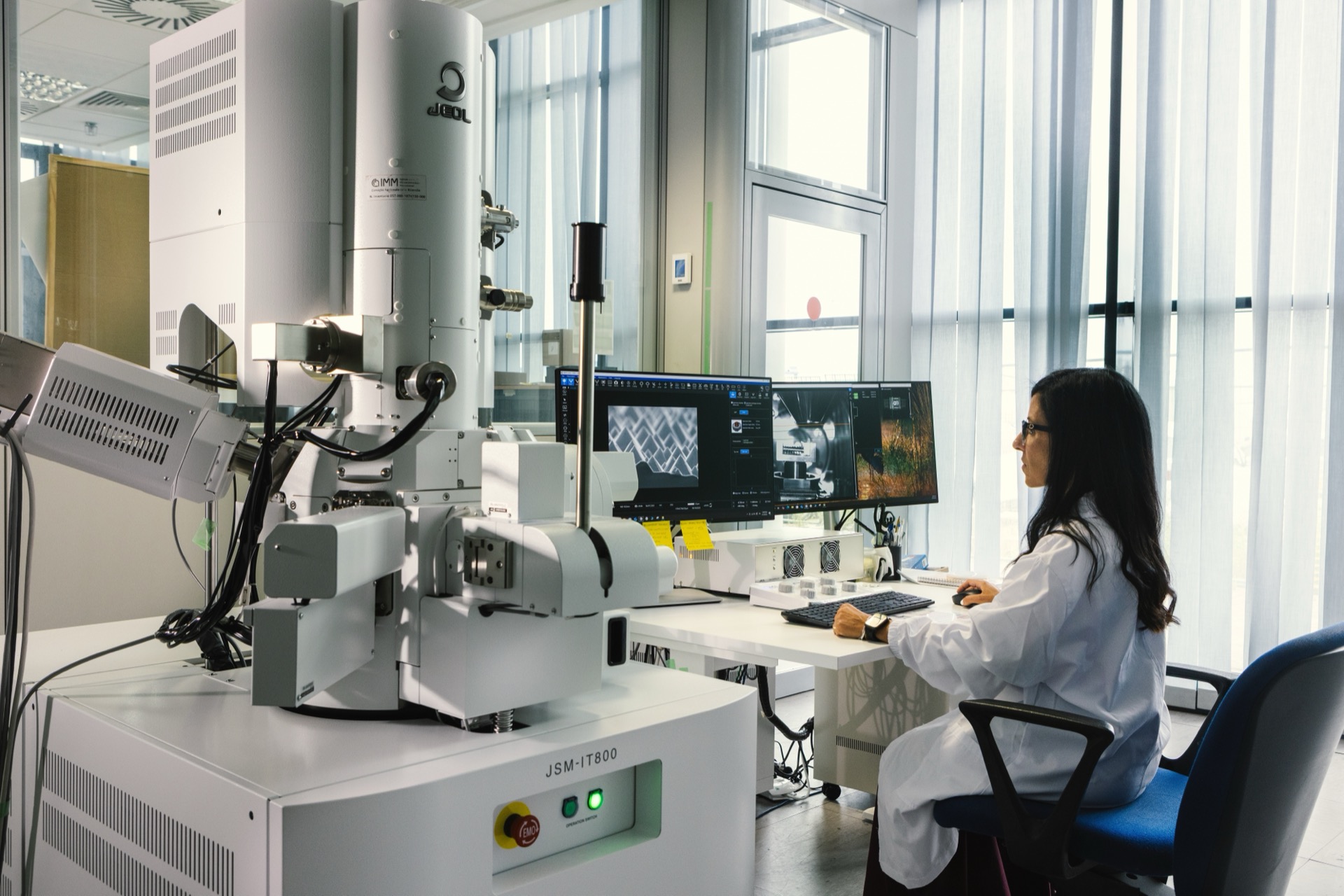
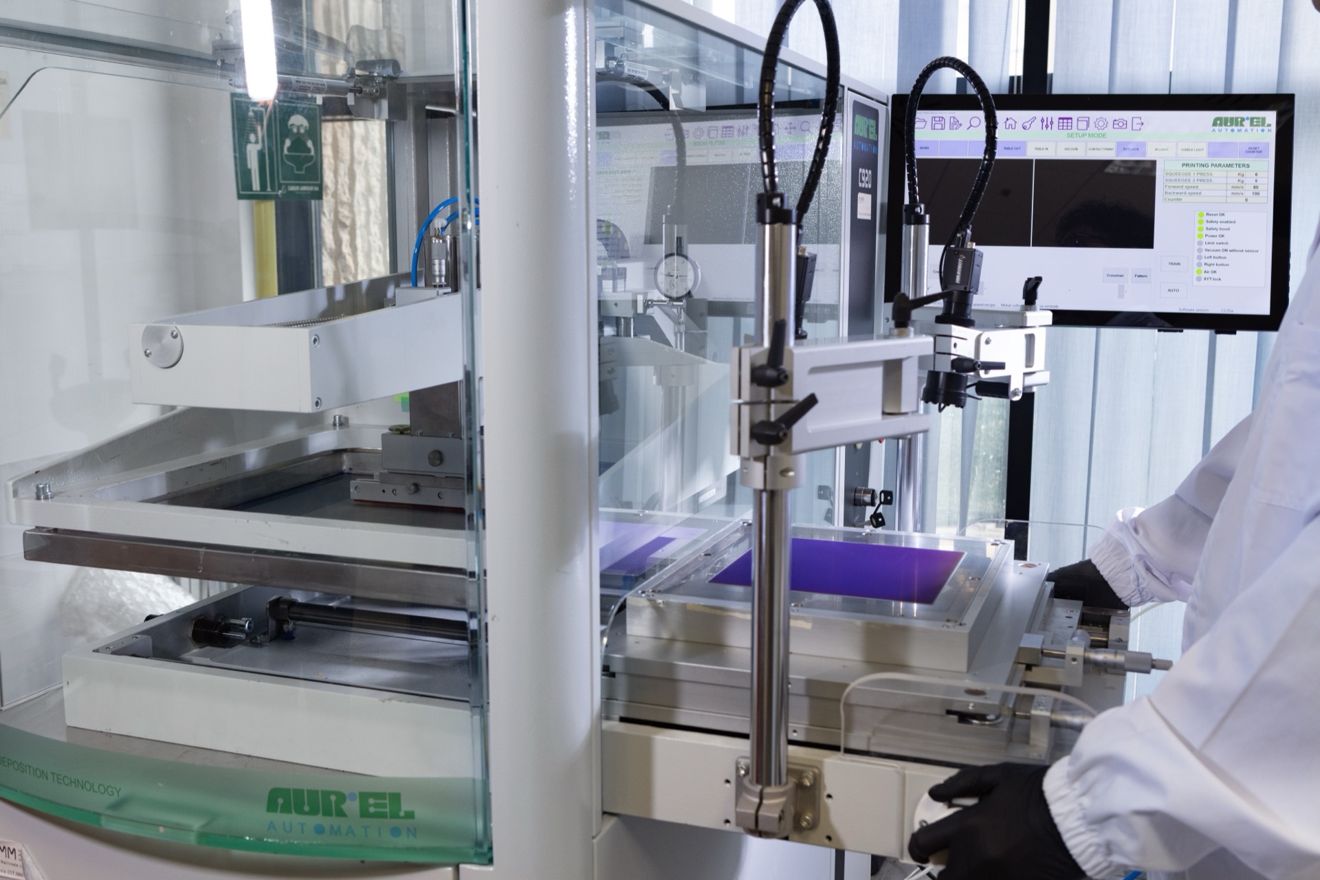
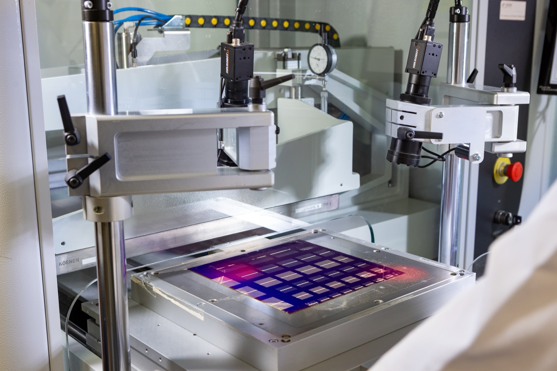
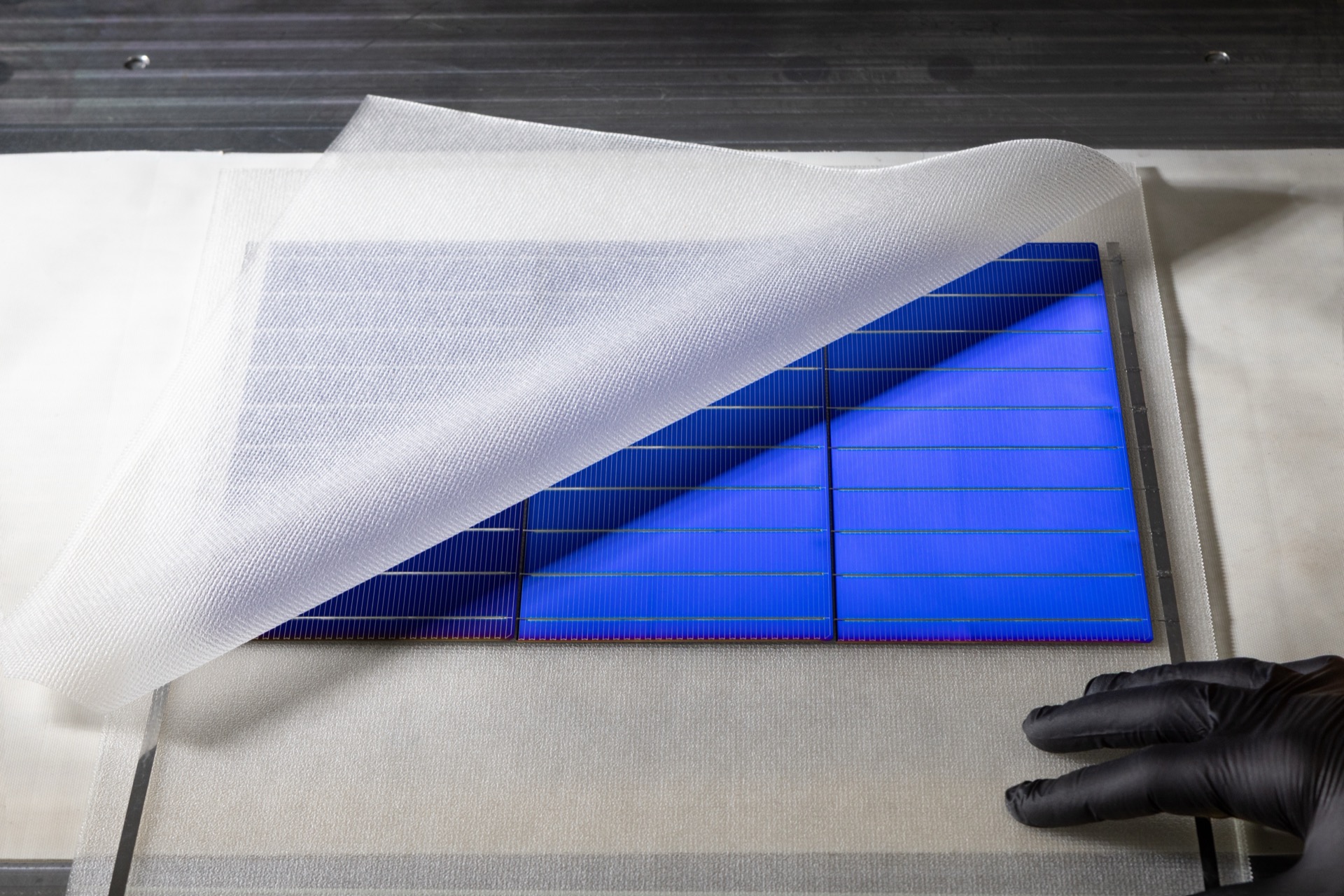
The Lab_Power&RF Facility of Beyond-Nano
The development of materials and processes for power and high-frequency devices based on wide band gap (WBG) semiconductors is at the core of the research conducted at Lab_Power&RF.
The main facilities of Lab_Power&RF facility are:

Clean Room
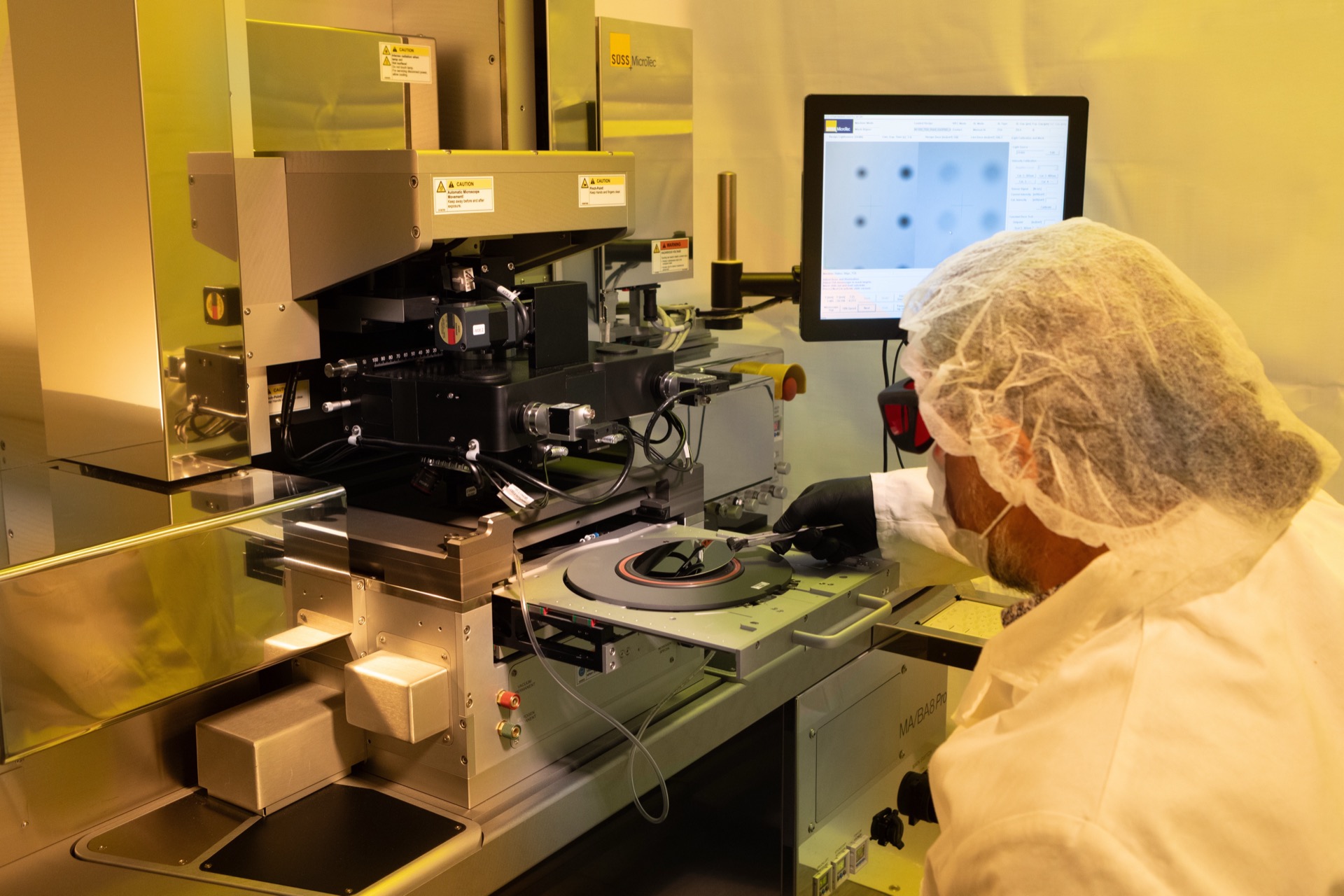
(300 m 2 , class ISO4) equipped for front-end fabrication of power and RF devices, test structures and novel devices based on WBG semiconductors and 2D materials (graphene and MoS 2 )

Metal Organic Chemical Vapor Deposition
(MOCVD) laboratory with a reactor for the
growth of different WBG epilayers and heterostructures

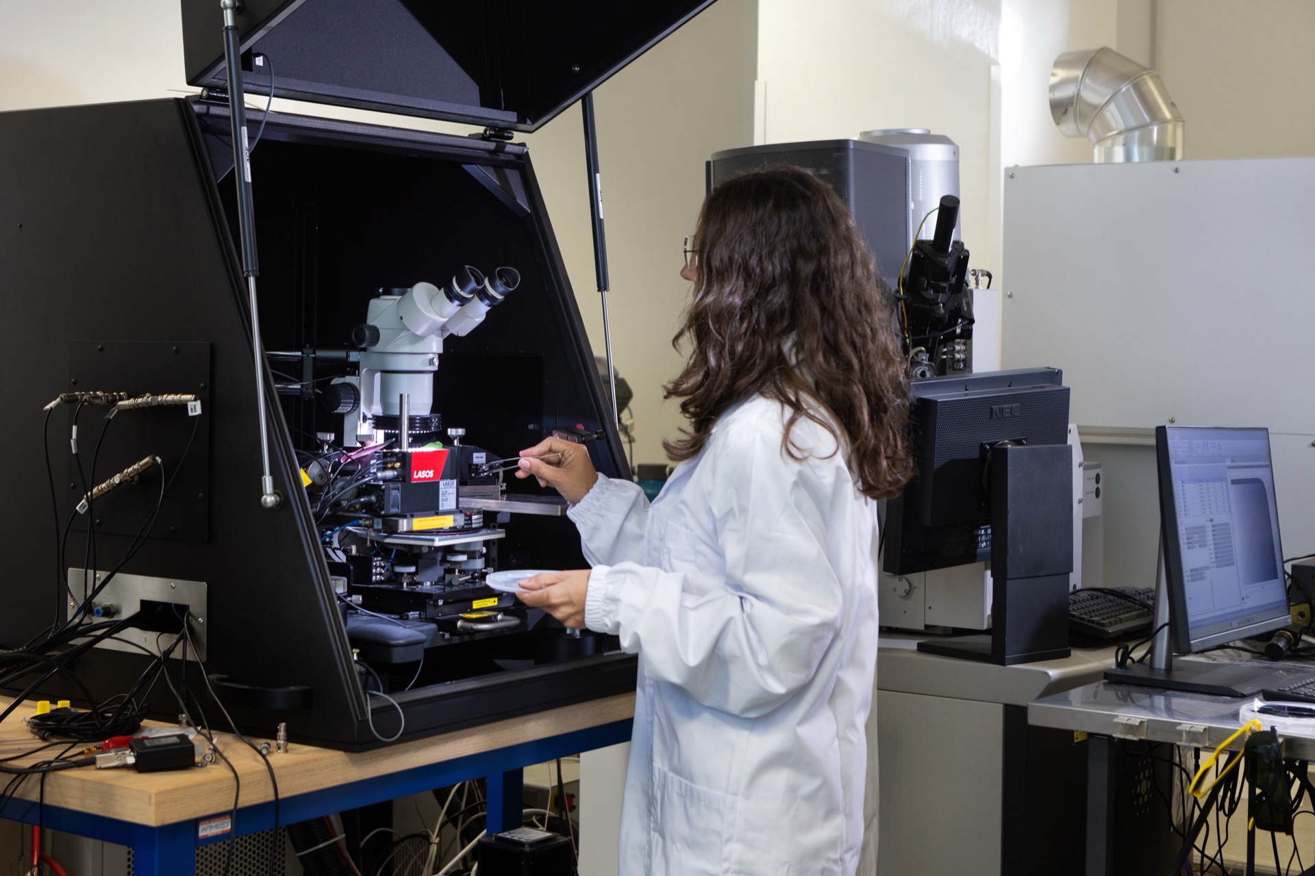
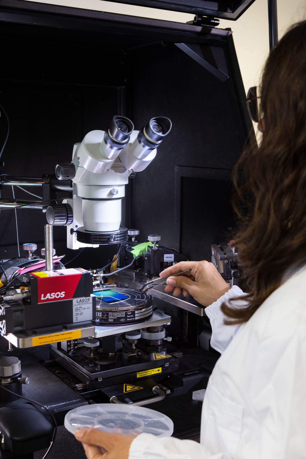
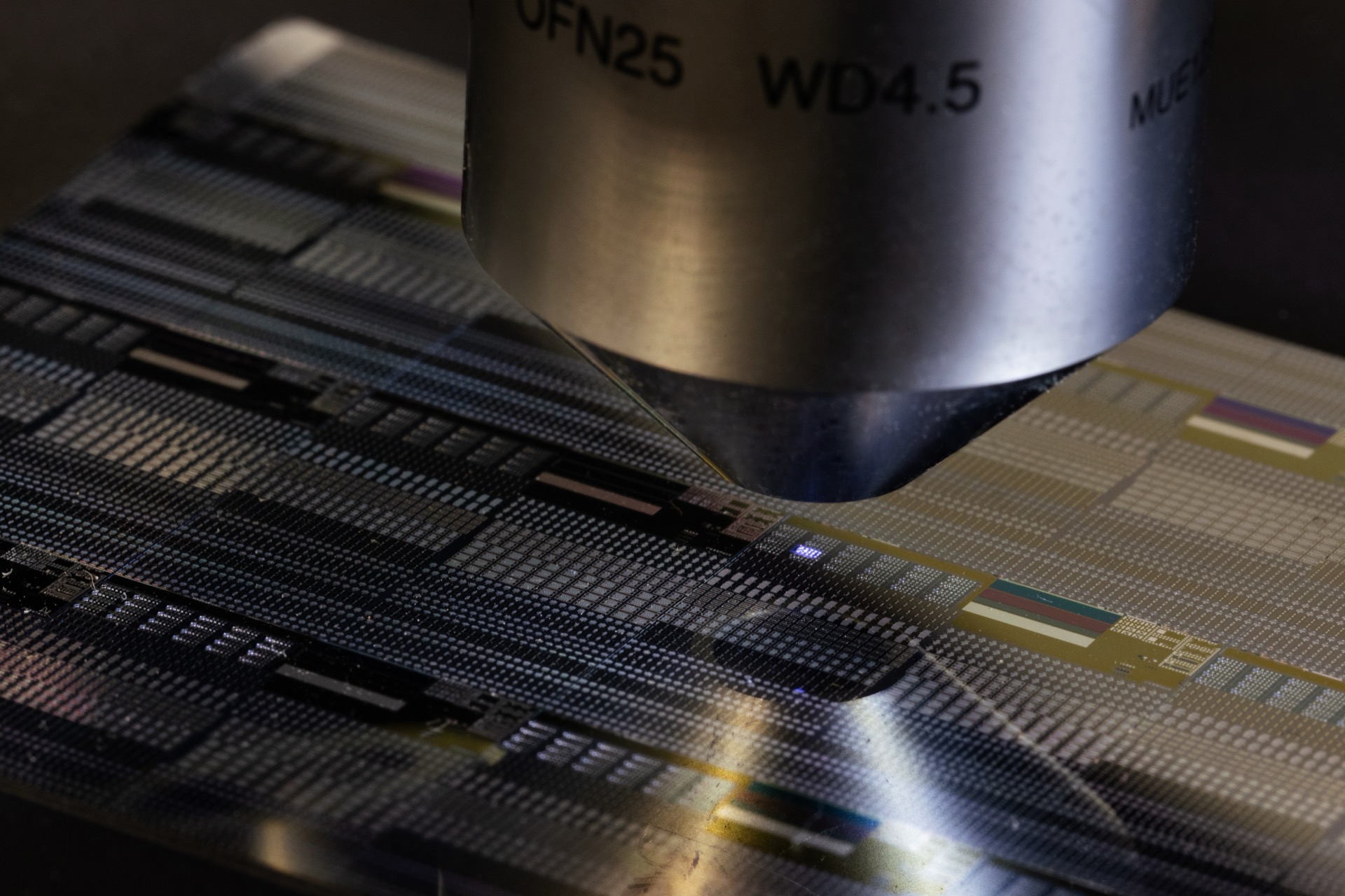
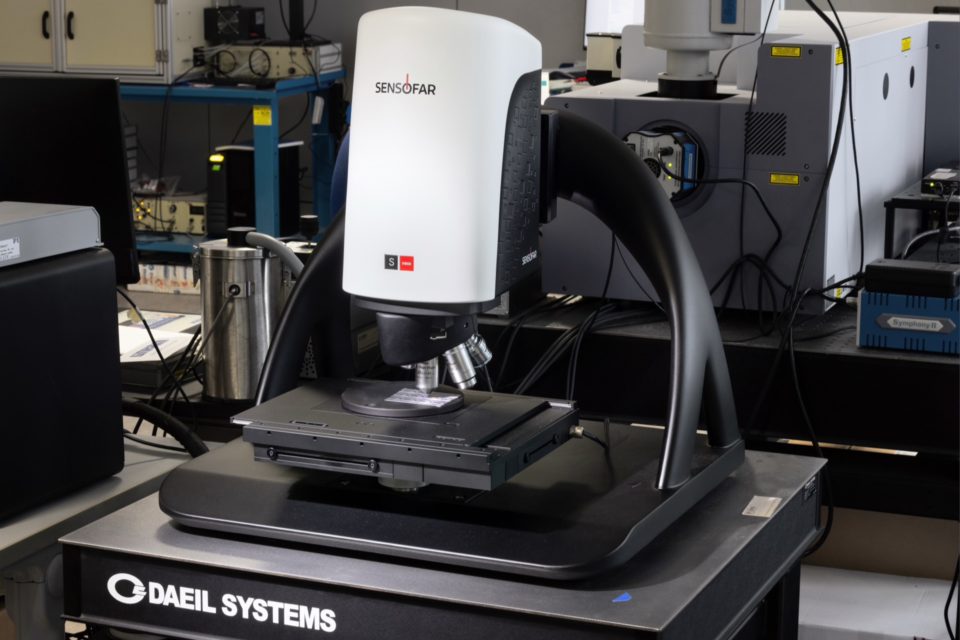
Advanced testing laboratory
with state-of-the-art facilities to characterize materials and devices with electro-optical methods
fields of application
The Lab_Power&RF facility within Beyond-Nano addresses several key scientific and technological challenges of SiC and GaN-based technologies. It also engages in frontier research focused on integrating 2D materials (such as graphene and MoS₂) with WBG semiconductors, and on developing technologies based on ultra-wide bandgap (UWBG) semiconductors, including gallium oxide (Ga₂O₃), aluminum nitride (AlN), and diamond.

Materials Growth
Nitrides growth on different substrates up to 200 mm in diameter, enabling the production of a wide range of epitaxial layers and heterostructures for lateral and vertical devices, as well as novel hybrid device architectures

Device Processing
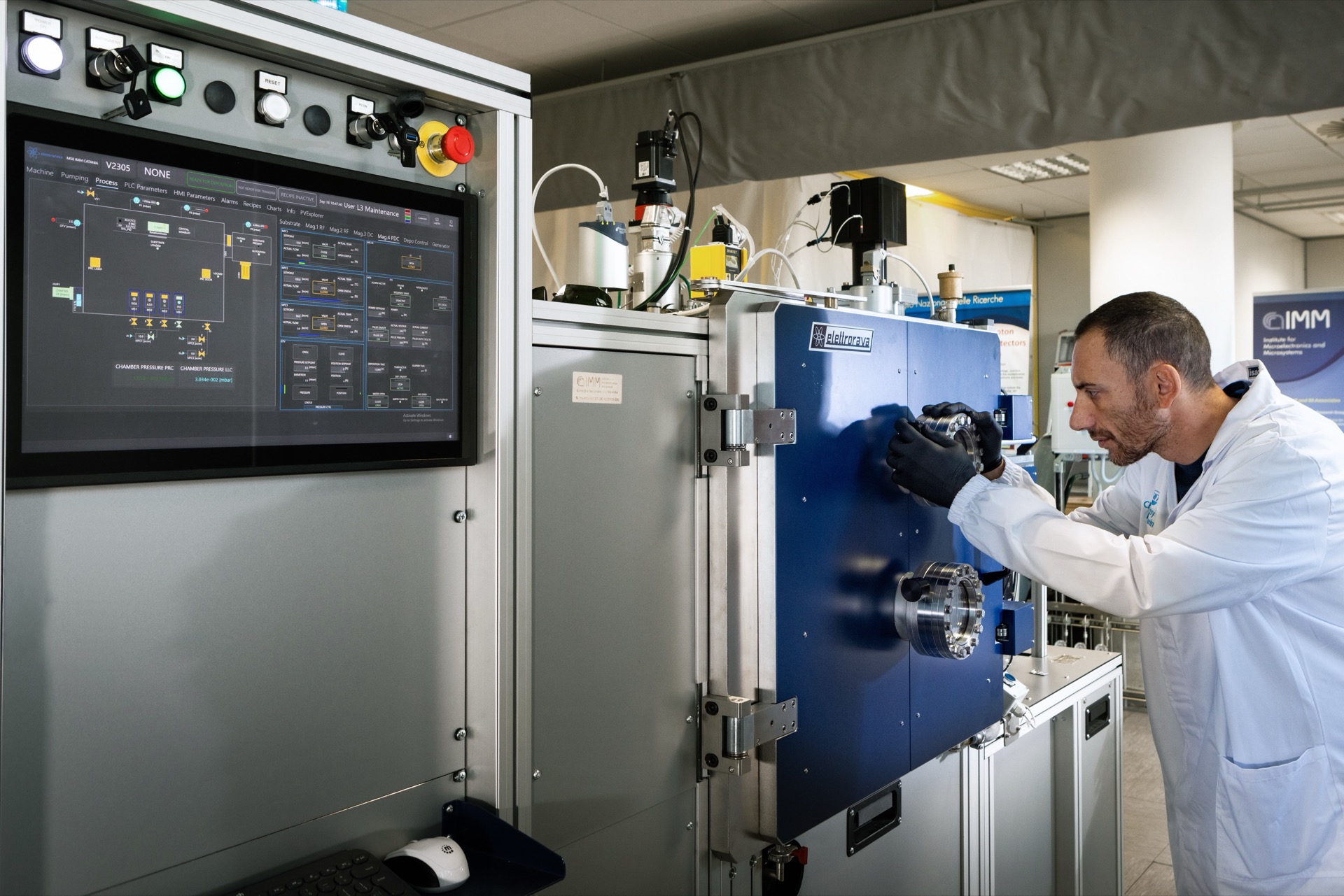
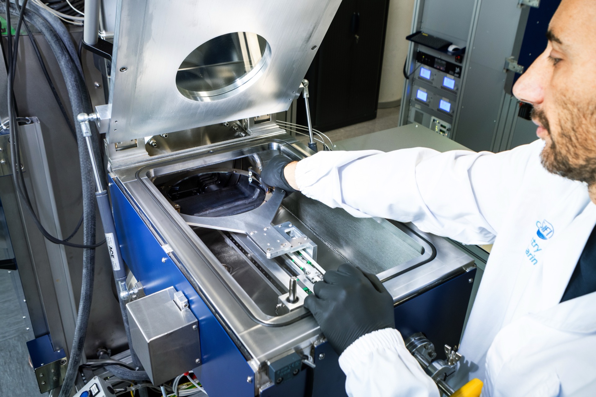
Process modules for WBG device technology on coupons and wafers up to 200 mm in diameter: lithography, metals evaporation/sputtering, atomic layer deposition (ALD), plasma etching, rapid and conventional annealing in different atmospheres (N2, O2, Ar, N2O) up to 2000 °C

Advanced Testing
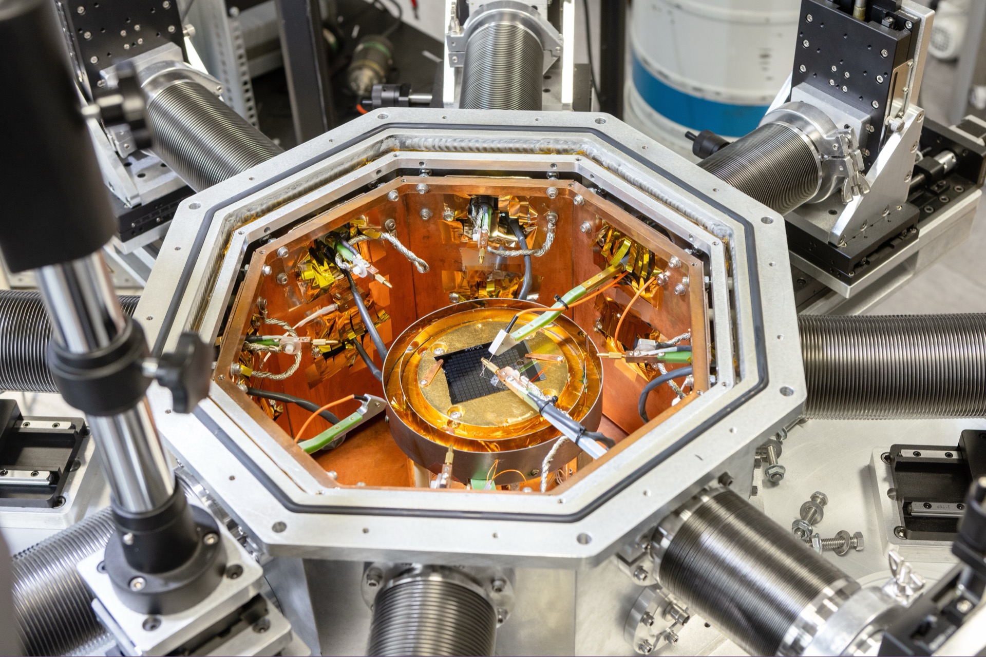
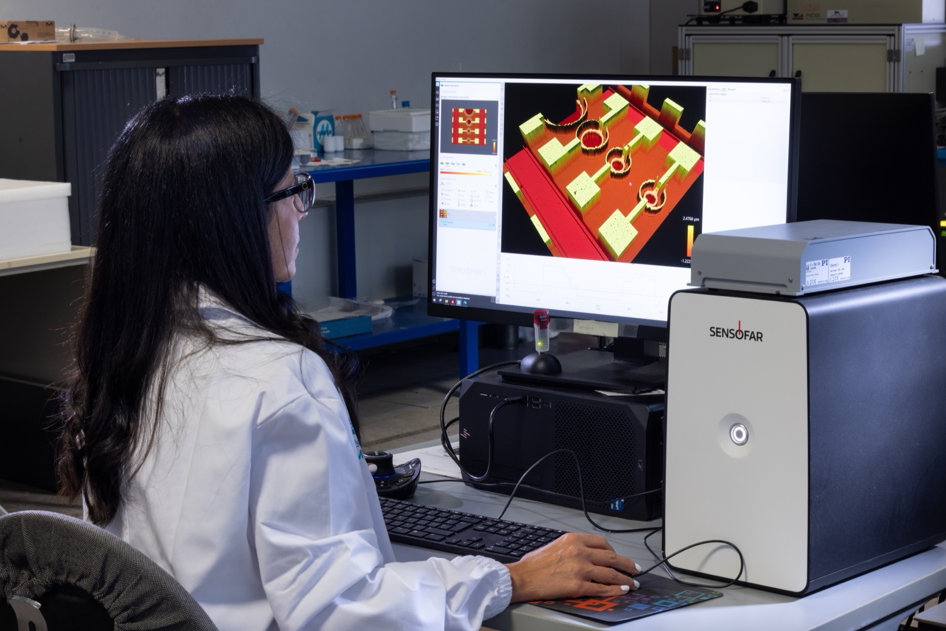
Electrical, thermal and electro-optical testing both at the device wafer-level and at the nanoscale, e.g. scanning probe microscopy (SPM)-based electrical/thermal characterizations combined with micro-Raman/PL
LAB_PV GALLERY